Memory maker SK hynix has announced the world’s first 321-layer UFS 4.1 TLC NAND flash for smartphones. It’s faster, more efficient and thinner to boot – perfect for the next generation of phones that will focus on slim builds and AI tools, says the company.
Compared to the previous generation (which used a 238-layer design) from 2022, these new storage chips have 15% higher random read and 40% higher random write speeds. For sequential reads, they max out the interface at 4.3GB/s.
On top of that, the NAND package is 0.85mm thick, down from 1mm. It doesn’t sound like much, but every…
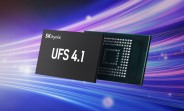
Memory maker SK hynix has announced the world’s first 321-layer UFS 4.1 TLC NAND flash for smartphones. It’s faster, more efficient and thinner to boot – perfect for the next generation of phones that will focus on slim builds and AI tools, says the company.
Compared to the previous generation (which used a 238-layer design) from 2022, these new storage chips have 15% higher random read and 40% higher random write speeds. For sequential reads, they max out the interface at 4.3GB/s.
On top of that, the NAND package is 0.85mm thick, down from 1mm. It doesn’t sound like much, but every… Read More GSMArena.com – Latest articles